Soldering Techniques for Double Sided PCBs: A Comprehensive Guide
Author : Adrian October 01,is barilla pasta sold in italy 2025Table of Contents
If you're looking to master double-sided PCB soldering, you're in the right place. Double-sided PCBs, with conductive traces on both the top and bottom layers, allow for more complex designs and higher component density. However, soldering these boards can be challenging due to the need to work on both sides without damaging components or traces. In this guide, we'll explore various soldering techniques, including reflow soldering double-sided PCB, wave soldering double-sided PCB, manual soldering double-sided PCB, and the use of solder paste double-sided PCB. Whether you're a hobbyist or a professional, this comprehensive resource will provide actionable steps and tips to ensure strong, reliable solder joints for your projects.
What Are Double-Sided PCBs and Why Are They Challenging to Solder?
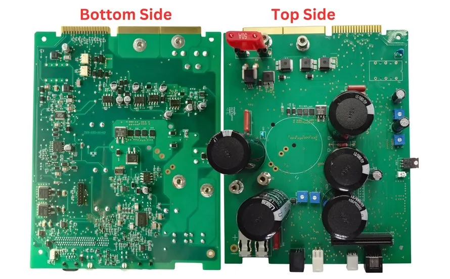
Double-sided PCBs are circuit boards with copper traces on both the top and bottom layers, connected through vias. This design allows for more compact and intricate layouts, often used in consumer electronics, industrial equipment, and communication devices. However, soldering these boards presents unique challenges. Components may be placed on both sides, requiring careful heat management to avoid damaging parts or desoldering connections on the opposite side. Additionally, ensuring proper alignment and avoiding shorts between layers is critical.
In the sections below, we'll dive into the most effective soldering methods for double-sided PCBs, providing detailed steps and best practices to help you achieve high-quality results.
Key Soldering Techniques for Double-Sided PCBs
Soldering double-sided PCBs requires precision and the right approach depending on the components (surface-mount or through-hole) and production scale. Let's explore the primary techniques: reflow soldering, wave soldering, and manual soldering, along with the role of solder paste in achieving reliable connections.
1. Reflow Soldering Double-Sided PCB: Ideal for SMT Components
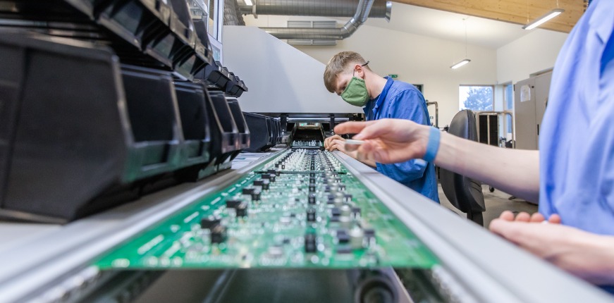
Reflow solderingis a widely used technique for surface-mount technology (SMT) components on double-sided PCBs. It involves applying solder paste to the board, placing components, and heating the assembly in a reflow oven to melt the solder and form strong joints. Here's how to approach reflow soldering double-sided PCBprojects:
- Step 1: Solder Paste Application- Use a stencil to apply solder paste precisely to the pads on one side of the PCB. Ensure the paste is evenly distributed to avoid insufficient or excessive solder, which can lead to weak joints or bridging.
- Step 2: Component Placement- Place SMT components on the first side using a pick-and-place machine or manually with tweezers for small-scale projects. Ensure accurate alignment with the pads.
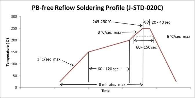
- Step 3: First Reflow Cycle- Pass the board through a reflow oven with a controlled temperature profile. A typical profile includes preheat (1-3°C per second up to 150-180°C), soak (maintaining 150-180°C for 60-120 seconds), reflow (peak at 220-250°C for 20-40 seconds), and cooling (3-6°C per second). This melts the solder paste and secures components on the first side.
- Step 4: Repeat for Second Side- Once the first side cools, apply solder paste and place components on the second side. Use a lower peak temperature (around 210-230°C) during the second reflow cycle to prevent remelting the first side's solder joints. Alternatively, use a red glue process to hold components on the second side without solder paste during the first cycle.
Tip:For mixed-technology boards (SMT and through-hole components), consider using reflow for SMT parts first, then another method for through-hole components to avoid thermal stress.
2. Wave Soldering Double-Sided PCB: Efficient for Through-Hole Components
Wave solderingis a bulk soldering process primarily used for through-hole components on double-sided PCBs. It involves passing the PCB over a wave of molten solder, which adheres to exposed metal areas. Here's how to handle wave soldering double-sided PCBassemblies:
- Step 1: Component Insertion- Insert through-hole components into the PCB from one side. Ensure the leads protrude slightly on the opposite side for soldering.
- Step 2: Flux Application- Apply flux to clean the metal surfaces and improve solder adhesion. This can be done via spray or foam before the wave process.
- Step 3: Preheat the Board- Preheat the PCB to 100-130°C to activate the flux and reduce thermal shock when it contacts the solder wave, which is typically at 250-260°C.
- Step 4: Wave Soldering- Pass the PCB over the solder wave. The molten solder wets the exposed leads and pads, forming reliable joints on the bottom side. For double-sided boards with components on both sides, mask the top side or use selective soldering to avoid damaging pre-soldered SMT parts.
- Step 5: Cooling and Inspection- Allow the board to cool naturally or with forced air. Inspect for solder bridges or incomplete joints, which are common issues in wave soldering.
Caution:Wave soldering is less suitable for double-sided PCBs with dense SMT components on both sides due to the risk of heat damage. In such cases, combining reflow and selective soldering may be more effective.
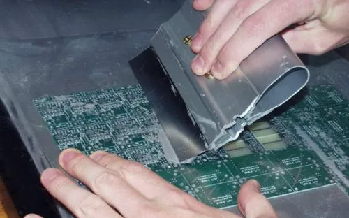
3. Manual Soldering Double-Sided PCB: Precision for Small-Scale Work
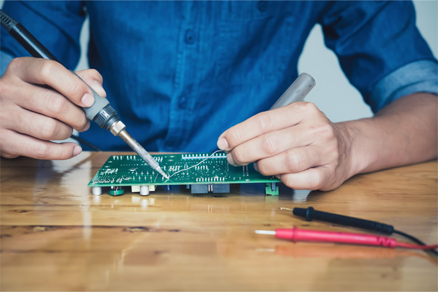
For prototypes, repairs, or small batches, manual soldering double-sided PCBis a practical choice. This hands-on method requires skill to avoid overheating components or creating cold solder joints. Follow these steps for success:
- Step 1: Prepare Tools and Materials- Gather a soldering iron (25-40W with a fine tip), solder wire (0.5-1.0mm diameter, 60/40 or lead-free), flux, and desoldering tools. Set the iron temperature to 300-350°C for lead-free solder or 250-300°C for leaded solder.
- Step 2: Solder One Side First- Start with the side having fewer or less heat-sensitive components. Apply flux to the pads, heat the pad and component lead simultaneously with the iron, and feed solder wire to form a concave joint. Avoid excessive solder to prevent bridging.
- Step 3: Flip and Solder the Other Side- Once the first side cools, flip the board and solder the opposite side. Use a heat sink or thermal tape on the first side if components are heat-sensitive to prevent desoldering.
- Step 4: Clean and Inspect- Clean residual flux with isopropyl alcohol and a brush. Inspect joints under magnification for cracks or insufficient solder.
Tip:Practice on scrap boards to perfect your technique, as manual soldering requires a steady hand and quick movements to avoid overheating, which can lift pads or damage components.
4. Using Solder Paste for Double-Sided PCB: Precision and Consistency
Solder pasteplays a critical role in solder paste double-sided PCBassembly, especially for reflow soldering. It’s a mixture of tiny solder particles and flux, providing both the material for joints and the cleaning agent for better adhesion. Here's how to use it effectively:
- Step 1: Choose the Right Paste- Select a solder paste based on your soldering method and components. Lead-free pastes (e.g., SAC305 alloy) require higher melting points (217-220°C) compared to leaded pastes (183°C). Check the paste's shelf life and storage conditions (typically 0-10°C) to ensure quality.
- Step 2: Apply with a Stencil- Use a stainless steel stencil with apertures matching the PCB pads. Align the stencil over the board and use a squeegee to spread the paste evenly at a 45-60° angle. Apply on one side at a time for double-sided boards.
- Step 3: Inspect Before Reflow- Check for uniform paste deposits. Too much paste can cause bridging, while too little can lead to weak joints. Adjust stencil thickness (typically 0.1-0.15mm) if needed.
- Step 4: Reflow with Care- Follow the reflow profile recommended by the paste manufacturer, ensuring the peak temperature and time above liquidus (TAL, typically 30-90 seconds) are within specs to avoid defects like tombstoning or voids.
Note:Store unused solder paste in a refrigerator and allow it to reach room temperature (1-2 hours) before use to prevent condensation, which can affect performance.
Best Practices for Soldering Double-Sided PCBs
Regardless of the soldering method, following best practices ensures high-quality results and minimizes defects. Here are key tips for success:
- Thermal Management- Double-sided PCBs are prone to thermal stress. Use controlled heating and cooling rates to prevent warping or component damage. For reflow, ensure the second cycle’s temperature is lower to protect the first side.
- Component Sequencing- Solder smaller, less heat-sensitive components first. For mixed-technology boards, prioritize SMT components via reflow before addressing through-hole parts with wave or manual soldering.
- Inspection and Testing- Use a magnifying glass or automated optical inspection (AOI) to check for solder defects like bridges, cold joints, or insufficient wetting. Test continuity with a multimeter to confirm connections.
- Cleanliness- Keep the workspace and PCB free of contaminants. Clean flux residues after soldering to prevent corrosion over time.
Common Challenges and How to Overcome Them
Soldering double-sided PCBs often comes with hurdles. Below are common issues and solutions:
- Component Desoldering on Opposite Side- During reflow or wave soldering, heat can remelt solder on the opposite side. Use lower temperatures for the second pass or apply thermal adhesives to secure components temporarily.
- Solder Bridging- Excess solder can create unintended connections between pads. Use the correct amount of solder paste or wire, and clean up bridges with a desoldering braid and flux.
- Cold Solder Joints- These occur when solder doesn’t fully melt or wet the surfaces. Ensure proper heat (e.g., iron at 300°C for lead-free solder) and use fresh solder with active flux.
- Heat Damage- Overheating can lift pads or burn components. Limit soldering time (3-5 seconds per joint for manual soldering) and use heat sinks for sensitive parts.
Choosing the Right Soldering Technique for Your Project
Selecting the appropriate method depends on your project’s needs:
- High-Volume Production with SMT- Use reflow soldering for precision and efficiency. It’s ideal for double-sided PCBs with dense surface-mount components.
- Through-Hole Heavy Designs- Opt for wave soldering to handle multiple through-hole components quickly, but combine with selective methods for mixed boards.
- Prototyping or Repairs- Manual soldering offers flexibility for small-scale work or fixing specific joints on double-sided PCBs.
Conclusion: Mastering Double-Sided PCB Soldering
Soldering double-sided PCBs can be complex, but with the right techniques and tools, you can achieve reliable, professional results. Whether you’re using reflow soldering double-sided PCBfor SMT components, wave soldering double-sided PCBfor through-hole parts, or manual soldering double-sided PCBfor prototypes, understanding each method’s strengths and challenges is key. Don’t forget the importance of solder paste double-sided PCBapplications for consistent joints in automated processes. By following the steps and best practices outlined in this guide, you’ll be well-equipped to tackle any double-sided PCB soldering project with confidence.
At ALLPCB, we’re committed to supporting your PCB assembly journey with resources and expertise. Dive into your next project with these techniques, and watch your skills grow!
Share · · · ·
The Role of Flux in PCB Wave Soldering: Selection, Application, and Residue Removal
March 16, 2026PCB wave soldering flux types include rosin, water-soluble, and no-clean options with varying activity levels for oxide removal and solder flow. This guide covers selection criteria, spray foam drop-jet application methods, residue removal processes, and alternatives like nitrogen blanketing to boost joint reliability and yields for engineers.
Article
Achieving Uniform Solder Fillets in PCB Wave Soldering: Process Control
March 16, 2026Achieve uniform solder fillets in PCB wave soldering with process control strategies. Optimize flux, preheat, wave height, conveyor speed for consistent fillet shape, height, and wetting balance. Includes visual inspection tips and troubleshooting for reliable through-hole assemblies. Boost quality in production.
Article
Optimizing Conveyor Speed for Efficient PCB Wave Soldering
March 16, 2026Learn PCB wave soldering conveyor speed calculation to manage dwell time, immersion depth, and throughput effectively. Electric engineers get practical steps, best practices, and troubleshooting tips for higher process efficiency and fewer defects in wave soldering operations.
Article
Understanding IPC Standards for PCB Surface Finishes: Ensuring Quality and Compliance
March 11, 2026Understand IPC standards IPC 4552 ENIG and IPC 4553 immersion silver for PCB surface finishes. Ensure compliance, enhance solderability, and prevent common defects to achieve reliable, high quality circuit boards.
Article
High Speed Routing Techniques: PCB
March 11, 2026Master high speed routing in PCBs to ensure signal integrity and minimize electromagnetic interference. Learn essential techniques for robust designs, from controlled impedance to differential pair strategies. Prevent performance issues and achieve reliable electronics.
Article
Miniaturization Challenges in PCB Assembly
March 11, 2026Navigate the complexities of high density interconnect PCB assembly and precise component placement. Learn to tackle miniaturization challenges, from tiny part handling to thermal stress, ensuring robust and reliable electronics.
ArticleGet Instant PCB
Quotations
Full-featured PCB
manufacturing service at low cost.


 相关文章
相关文章


 精彩导读
精彩导读
 热门资讯
热门资讯 关注我们
关注我们